|
Full Stack
Now that we covered each layer of LTE protocol stack, it is time to combine all these layers to a complete protocol stack.
Try to follow the sequence below and combine all the knowledges you have and try to make practical sense out of it. This kind of integration is something not explanined in 3GPP specification and you have to figure out on your own.
Couple of bullet points for you to follow up are as follows :
- i) Which of the sequence requires normal MAC header and which of them does not use any MAC header ?
- ii) What is the practical meaning of "No MAC Header" and "Normal MAC Header" ?
- iii) Which process use RLC TM mode ? Which Process use RLC UM mode and Which process use RLC AM mode ?
- iv) Can you explain the detailed RLC layer behavior of each processes which is using RLC layer ?
- v) Which process use PDCP and which does not ?
|
Step
|
Direction
|
Channel
|
Message
|
|
1
|
UE <---- NW
|
BCCH -> BCH,
No MAC Header,RLC TM, No PDCP
|
MIB
|
|
2
|
UE <---- NW
|
BCCH -> DL SCH,
No MAC Header,RLC TM, No PDCP
|
SIBs
|
|
3
|
UE ----> NW
|
PRACH -> RACH,
No MAC Header,No RLC, No PDCP
|
PRACH Preamble
|
|
4
|
UE <---- NW
|
RACH -> DL SCH,
No MAC Header,No RLC, No PDCP
|
RACH Response
|
|
5
|
UE ----> NW
|
UL SCH -> UL CCCH
MAC Header,No RLC, No PDCP
|
RRC Connection Request
|
|
6
|
UE <---- NW
|
DL CCCH -> DL SCH
MAC Header,No RLC, No PDCP
|
RRC Connection Setup
|
|
7
|
UE ----> NW
|
UL SCH -> UL DCCH
MAC Header,RLC AM, PDCP
|
RRC : RRC Connection Setup Complete +
NAS : Attach Request (ESM:PDN Connectivity Request)
|
|
8
|
UE <---- NW
|
DL DCCH -> DL SCH
MAC Header,RLC AM, PDCP
|
RRC : dlInformationTransfer
EMM : Authentication Request
|
|
9
|
UE ----> NW
|
UL SCH -> UL DCCH
MAC Header,RLC AM, PDCP
|
RRC : ulInformationTransfer
EMM : Authentication Response
|
|
10
|
UE <---- NW
|
DL DCCH -> DL SCH
MAC Header,RLC AM, PDCP
|
RRC : dlInformationTransfer
EMM : Security Mode Command
|
|
11
|
UE ----> NW
|
UL SCH -> UL DCCH
MAC Header,RLC AM, PDCP
|
RRC : ulInformationTransfer
EMM : Security Mode Complete
|
|
12
|
UE <---- NW
|
DL DCCH -> DL SCH
MAC Header,RLC AM, PDCP
|
RRC : Security Mode Command
|
|
13
|
UE ----> NW
|
UL SCH -> UL DCCH
MAC Header,RLC AM, PDCP
|
RRC : Security Mode Complete
|
|
14
|
UE <---- NW
|
DL DCCH -> DL SCH
MAC Header,RLC AM, PDCP
|
RRC : RRC Connection Reconfiguration
EMM : Attach Accept
ESM : Activate Default EPS Bearer Context Request
|
|
15
|
UE ----> NW
|
UL SCH -> UL DCCH
MAC Header,RLC AM, PDCP
|
RRC : RRC Connection Reconfiguration Complete
|
|
16
|
UE ----> NW
|
UL SCH -> UL DCCH
MAC Header,RLC AM, PDCP
|
RRC : ulDirectTransfer
EMM : Attach Complete
ESM : Activate Default EPS Bearer Context Accept
|
|
17
|
UE <---- NW
|
DL DCCH -> DL SCH
MAC Header,RLC AM, PDCP
|
RRC : RRC Connection Release
|
NOTE : You can double check on these configuration in 36.331 summarized in SRB page.
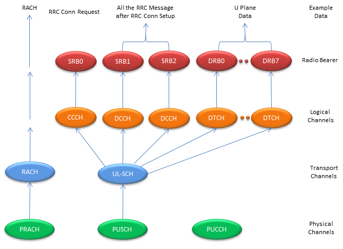
The diagram you saw above a kind of message flow(event diagram) in time sequence. The diagram shown below is not a time based, but it shows the channel mapping (or data flow across the full protocol stack). Pick one of the message from the diagram shown above and try to find right route for this digram and see how much details you can add.
For example, if you picked the message "RRC Connection Setup", the start point would be "RRC Message msg4".
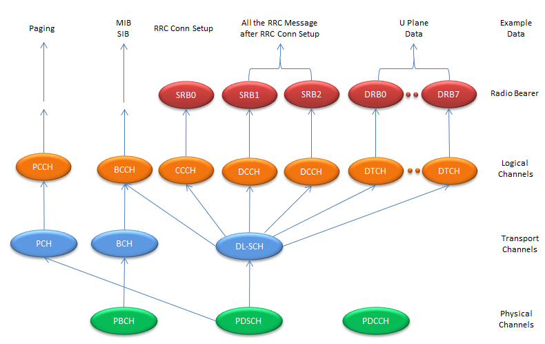
Following is a tabular presentation of DL Channel Map. (LCID and TrCH Number would be different depending on the network or Network Simulator)
|
RB
|
Lo CH
|
PDCP
|
RLC
|
Lo CH
|
LCID
|
MAC Hdr
|
HARQ
|
RNTI
|
Tr CH
|
|
|
PCCH
|
|
TM
|
PCCH
|
N/A
|
NONE
|
NONE
|
NONE
|
PCH
|
|
|
BCCH 0
|
|
TM
|
BCCH 0
|
N/A
|
NONE
|
NONE
|
NONE
|
BCH 0
|
|
|
BCCH 1
|
|
TM
|
BCCH 1
|
N/A
|
NONE
|
Broadcast
|
SI RNTI
|
DL SCH 0
|
|
|
RA_RES
|
|
TM
|
RA_RES
|
N/A
|
NONE
|
NONE
|
RA RNTI
|
DL SCH 1
|
|
SRB0
|
DL CCCH
|
USED
|
TM
|
DL CCCH
|
0
|
NONE
|
NORMAL
|
T-CRNTI
|
DL SCH 1
|
|
SRB1
|
DL DCCH 0
|
USED
|
AM
|
DL DCCH 0
|
1
|
NORMAL
|
NORMAL
|
CRNTI
|
DL SCH 1
|
|
SRB2
|
DL DCCH 1
|
USED
|
AM
|
DL DCCH 0
|
2
|
NORMAL
|
NORMAL
|
CRNTI
|
DL SCH 1
|
|
DRB 0
|
DL DTCH0
|
USED
|
UM/AM
|
DL DTCH0
|
3
|
NORMAL
|
NORMAL
|
CRNTI
|
DL SCH 1
|
|
DRB 1
|
DL DTCH0
|
USED
|
UM/AM
|
DL DTCH0
|
4
|
NORMAL
|
NORMAL
|
CRNTI
|
DL SCH 1
|
|
DRB 2
|
DL DTCH0
|
USED
|
UM/AM
|
DL DTCH0
|
5
|
NORMAL
|
NORMAL
|
CRNTI
|
DL SCH 1
|
Following is a tabular presentation of DL Channel Map. (LCID and TrCH Number would be different depending on the network or Network Simulator)
|
RB
|
Lo CH
|
PDCP
|
RLC
|
Lo CH
|
LCID
|
MAC Hdr
|
HARQ
|
RNTI
|
Tr CH
|
|
|
RA_PRE
|
|
TM
|
RA_PRE
|
N/A
|
NONE
|
NONE
|
NONE
|
UL SCH 0
|
|
SRB0
|
UL CCCH
|
USED
|
TM
|
UL CCCH
|
0
|
NONE
|
NORMAL
|
T-CRNTI
|
UL SCH 0
|
|
SRB1
|
UL DCCH 0
|
USED
|
AM
|
UL DCCH 0
|
1
|
NORMAL
|
NORMAL
|
CRNTI
|
UL SCH 0
|
|
SRB2
|
UL DCCH 1
|
USED
|
AM
|
UL DCCH 0
|
2
|
NORMAL
|
NORMAL
|
CRNTI
|
UL SCH 0
|
|
DRB 0
|
UL DTCH0
|
USED
|
UM/AM
|
UL DTCH0
|
3
|
NORMAL
|
NORMAL
|
CRNTI
|
UL SCH 0
|
|
DRB 1
|
UL DTCH0
|
USED
|
UM/AM
|
UL DTCH0
|
4
|
NORMAL
|
NORMAL
|
CRNTI
|
UL SCH 0
|
|
DRB 2
|
UL DTCH0
|
USED
|
UM/AM
|
UL DTCH0
|
5
|
NORMAL
|
NORMAL
|
CRNTI
|
UL SCH 0
|
This is only an example case and Mapping (especiall LoCH No) can vary depending on situations. The point is that it will be really helpful for your troubleshooting or test case creation if you create this kind of table for your case.
|
Message
|
RB
|
Lo CH
|
LoCH No
|
LCID
|
|
MIB
|
-
|
BCCH
|
0
|
-
|
|
SIB 1
|
-
|
BCCH
|
1
|
-
|
|
SIB 2
|
-
|
BCCH
|
1
|
-
|
|
RRC : PRACH Preamble
|
-
|
-
|
-
|
-
|
|
RRC : RACH Response
|
-
|
-
|
-
|
-
|
|
RRC : RRC Connection Request
|
SRB0
|
UL CCCH
|
0
|
0
|
|
RRC : RRC Connection Setup
|
SRB0
|
DL CCCH
|
0
|
0
|
|
RRC : RRC Connection Setup
Complete + NAS : Attach Request + ESM : PDN Connectivity Request
|
SRB1
|
UL DCCH
|
0
|
1
|
|
RRC : DL Information Transfer
+ NAS : Authentication Request
|
SRB1
|
DL DCCH
|
0
|
1
|
|
RRC : UL Information Transfer
+ NAS : Authentication Response
|
SRB1
|
UL DCCH
|
0
|
1
|
|
RRC : DL Information Transfer
+ NAS : Security Mode Command
|
SRB1
|
DL DCCH
|
0
|
1
|
|
RRC : UL Information Transfer
+ NAS : Security Mode Complete
|
SRB1
|
UL DCCH
|
0
|
1
|
|
RRC : Security Mode Command
|
SRB1
|
DL DCCH
|
0
|
1
|
|
RRC : Security Mode Complete
|
SRB1
|
UL DCCH
|
0
|
1
|
|
RRC : RRC Connection
Reconfiguration
|
SRB1
|
DL DCCH
|
0
|
1
|
|
RRC
: RRC Connection Reconfiguration Complete
|
SRB1
|
UL DCCH
|
0
|
1
|
|
RRC
: UL InformationTransfer + NAS : Attach Complete + NAS : Activate Default EPS
Bearer
|
SRB2
|
UL DCCH
|
1
|
2
|
|
RRC : UL Information Transfer
+ ESM : PDN Connectivity Request
|
SRB2
|
UL DCCH
|
1
|
2
|
Note : Refer to TS 36.331 - 9.1.1 Logical channel configurations
This can a good example in which you can practice on very details of MAC to PDCP in detail. This is a segment of logs between a UE and a live network, meaning it shows what's happening in real network. I captured a log using Intellijudge and Wavejudge from SanJole and reformated so that it is easier to read. (First understand the details of RACH, MAC, PDCP in detail especially about the data structure of each layer and then revisit this and see how much you can make sense out of this).
|
SFN : 402.4
|
RACH Preamble
|
|
|
RNTI = None
Timing Offset = 2
Logical Root = 219
Preamble index = 33
NC Configuration = 12
Set Type = Unrestricted
Logical Root = 215
Preamble Format = 0
RbStart = 2
|
|
SFN : 402.8
|
MAC RA Response
|
|
|
MAC : 61 00 B0 C0 4C 2C 09
E = 0(False)
T = 1
RAPID = 33
Timing Advanced = 11
Hopping Flag 0 = False
Fixed Size Resource Block Assignment = 96 (RB Start = 46, RB Length = 2)
MCS = 2, I_TBS = 2, rv = 0
TPC Command for PUCCH 3 = 0
UL Delay 0 = False
CQI Request = False
T_CRNTI = 11273
|
|
SFN : 403.4
|
PUSCH - RRC Connection Request
|
|
|
MAC : 20 06 1F 5C 2C 04 B2 AC F6
Sub Header 0
R = OK
E = 1
LCID = 0 (CCCH)
F = 0 (False)
L = 6
Sub Header 1
R = OK
E = 0
LCID = 31 (Padding)
CCCH-RLC : 5C 2C 04 B2 AC F6 (RRC Connection Request)
|
|
SFN : 403.8
|
PHICH-ACK
|
|
|
|
|
SFN : 404.7
|
PDCCH (DCI Format 1) + PDSCH (RRC Connection Setup)
|
|
|
CCE Start = 0
CCE Length = 8
DCI Format 1A (Hex : 47D01E2)
Format = 1
Distributed VRB flag = 0 (Local)
Resource Allocation = 500 (RB Start = 0, RB Length = 11)
MCS = 0 (I_TBS = 0)
HARQ Process Number = 7
NDI (New Data Indicator) = 1 (True)
RV = 0
TPC Command for PUCCH = 1
MAC : 3C 20 1A 1F 5C 2C 04 B2 AC F6 60 12 98 08 FD 4E .....
Sub Header 0
R = OK
E = 1
LCID = 28 (UE Contention Resolution Identity)
Sub Header 1
R = OK
E = 1
LCID = 1 (CCCH)
F = 0 (False)
L = 26
Sub Header 2
R = OK
E = 0
LCID = 31 (Padding)
UE Contention Resolution Identity
|
|
SFN : 405.1
|
PUCCH - UCI HARQ ACK
|
|
|
PUCCH Format 1 A
n PUCCH = 16
|
|
SFN : 406.2
|
PUCCH - UCI SR
|
|
|
N PUCCH RB = 2
|
|
SFN : 406.6
|
PDCCH - DCI Format 0
|
|
|
PDCCH DCI Format 0 (Hex : 0180540)
Format 0
Hopping Flag = 0 (False)
RB Allocation of 1st Slot in UL subframe = 96
MCS 2, RV 0
NDI = 1 (True)
TPC = 1
Cyclic Shift for DMRS = 0
CQI Requested = 0 (False)
|
|
SFN : 406.7
|
PDCCH - DCI Format 0
|
|
|
DCI Format 0 (Hex : 0180540)
Format 0
Hopping Flag = 0 (False)
RB Allocation of 1st Slot in UL subframe = 96
MCS 2, RV 0
NDI = 1 (True)
TPC = 1
Cyclic Shift for DMRS = 0
CQI Requested = 0 (False)
|
|
SFN : 406.8
|
PDCCH - DCI Format 0
|
|
|
DCI Format 0 (Hex : 0180540)
Format 0
Hopping Flag = 0 (False)
RB Allocation of 1st Slot in UL subframe = 96
MCS 2, RV 0
NDI = 1 (True)
TPC = 1
Cyclic Shift for DMRS = 0
CQI Requested = 0 (False)
|
|
SFN : 406.9
|
PDCCH - DCI Format 0
|
|
|
DCI Format 0 (Hex : 0180540)
Format 0
Hopping Flag = 0 (False)
RB Allocation of 1st Slot in UL subframe = 96
MCS 2, RV 0
NDI = 1 (True)
TPC = 1
Cyclic Shift for DMRS = 0
CQI Requested = 0 (False)
|
|
SFN : 407.0
|
PDCCH - DCI Format 0
|
|
|
DCI Format 0 (Hex : 0180540)
Format 0
Hopping Flag = 0 (False)
RB Allocation of 1st Slot in UL subframe = 96
MCS 2, RV 0
NDI = 1 (True)
TPC = 1
Cyclic Shift for DMRS = 0
CQI Requested = 0 (False)
|
|
SFN : 407.0
|
PUSCH - RRC Connection Setup Complete (First Segment)
|
|
|
MAC = 3A 3D 01 22 10 88 00 00 20
Sub Header 0
R = OK
E = 1
LCID = 26 (Power Headroom Report)
Sub Header 1
R = OK
E = 1
LCID = 29 (Short Buffer Status Report)
Sub Header 2
R = OK
E = 0
LCID = 1 (identity)
Power Headroom
R = OK
Power Headroom --> 11 dB <= PH <= 12 dB
Short Buffer Status Report
LCG ID = 0
Buffer Size 16 --> 91 < BS <= 107
RLC AMD = 88 00 00 20
D/C = 1 (Data PDU)
RF = 0 (AMD PDU)
P = 0 (Status Report Not Requested)
Fl = 1 (First Byte of the Data Field corresponds to the first byte of a RLC SDU. Last byte of Data field does not corresponds to the last byte of a RLC PDU)
E = 0 (False)
SN = 0
PDCP-CP-SRB = 00 20
|
|
SFN : 407.1
|
PUSCH - RRC Connection Setup Complete (Mid Segment)
|
|
|
MAC = 01 98 01 20 80 01 00 59 17
Sub Header 0
R = OK
E = 0
LCID = 1 (identity)
RLC AMD = 98 01 20 80 01 00 59 17
D/C = 1 (Data PDU)
RF = 0 (AMD PDU)
P = 0 (Status Report Not Requested)
Fl = 3 (First Byte of the Data Field does not corresponds to the first byte of a RLC SDU.
Last byte of Data field does not corresponds to the last byte of a RLC PDU)
E = 0 (False)
SN = 1
PDCP-CP-SRB = 20 80 01 00 59 17
|
|
SFN : 407.1
|
PDCCH - DCI Format 0
|
|
|
DCI Format 0 (Hex : 0180540)
Format 0
Hopping Flag = 0 (False)
RB Allocation of 1st Slot in UL subframe = 96
MCS 2, RV 0
NDI = 1 (True)
TPC = 1
Cyclic Shift for DMRS = 0
CQI Requested = 0 (False)
|
|
SFN : 407.1
|
PUSCH - RRC Connection Setup Complete (Mid Segment)
|
|
|
MAC = 01 98 02 39 45 E5 34 0B 07
Sub Header 0
R = OK
E = 0
LCID = 1 (identity)
RLC AMD = 98 02 39 45 E5 34 0B 07
D/C = 1 (Data PDU)
RF = 0 (AMD PDU)
P = 0 (Status Report Not Requested)
Fl = 3 (First Byte of the Data Field does not corresponds to the first byte of a RLC SDU. Last byte of Data field does not corresponds to the last byte of a RLC PDU)
E = 0 (False)
SN = 2
PDCP-CP-SRB = 39 45 E5 34 0B 07
|
|
SFN : 407.2
|
PDCCH - DCI Format 0
|
|
|
DCI Format 0 (Hex : 0180540)
Format 0
Hopping Flag = 0 (False)
RB Allocation of 1st Slot in UL subframe = 96
MCS 2, RV 0
NDI = 1 (True)
TPC = 1
Cyclic Shift for DMRS = 0
CQI Requested = 0 (False)
|
|
SFN : 407.3
|
PUSCH - RRC Connection Setup Complete (Mid Segment)
|
|
|
MAC = 01 98 02 41 02 0B F6 03 02
Sub Header 0
R = OK
E = 0
LCID = 1 (identity)
RLC AMD = 98 03 41 02 0B F6 03 02
D/C = 1 (Data PDU)
RF = 0 (AMD PDU)
P = 0 (Status Report Not Requested)
Fl = 3 (First Byte of the Data Field does not corresponds to the first byte of a RLC SDU. Last byte of Data field does not corresponds to the last byte of a RLC PDU)
E = 0 (False)
SN = 3
PDCP-CP-SRB = 41 02 0B F6 03 02
|
|
SFN : 407.3
|
PDCCH - DCI Format 0
|
|
|
DCI Format 0 (Hex : 0180540)
Format 0
Hopping Flag = 0 (False)
RB Allocation of 1st Slot in UL subframe = 96
MCS 2, RV 0
NDI = 1 (True)
TPC = 1
Cyclic Shift for DMRS = 0
CQI Requested = 0 (False)
|
|
SFN : 407.4
|
PHICH ACK
|
|
|
....
|
|
SFN : 407.4
|
PDCCH - DCI Format 0
|
|
|
DCI Format 0 (Hex : 0180440)
Format 0
Hopping Flag = 0 (False)
RB Allocation of 1st Slot in UL subframe = 96
MCS 2, RV 0
NDI = 0 (False)
TPC = 1
Cyclic Shift for DMRS = 0
CQI Requested = 0 (False)
|
|
SFN : 407.4
|
PUSCH - RRC Connection Setup Complete (Mid Segment)
|
|
|
MAC = 01 98 04 27 80 01 00 D0 CC
Sub Header 0
R = OK
E = 0
LCID = 1 (identity)
RLC AMD = 98 04 27 80 01 00 D0 CC
D/C = 1 (Data PDU)
RF = 0 (AMD PDU)
P = 0 (Status Report Not Requested)
Fl = 3 (First Byte of the Data Field does not corresponds to the first byte of a RLC SDU. Last byte of Data field does not corresponds to the last byte of a RLC PDU)
E = 0 (False)
SN = 4
PDCP-CP-SRB = 27 80 01 00 D0 CC
|
|
SFN : 407.5
|
PUSCH - RRC Connection Setup Complete (Mid Segment)
|
|
|
MAC = 3D 01 0E 98 05 71 51 04 E0
Sub Header 0
Sub Header 1
R = OK
E = 0
LCID = 1 (identity)
Short Buffer Status Report
RLC AMD = 98 05 71 51 04 E0
D/C = 1 (Data PDU)
RF = 0 (AMD PDU)
P = 0 (Status Report Not Requested)
Fl = 3 (First Byte of the Data Field does not corresponds to the first byte of a RLC SDU. Last byte of Data field does not corresponds to the last byte of a RLC PDU)
E = 0 (False)
SN = 5
PDCP-CP-SRB = 71 51 04 E0
|
|
SFN : 407.5
|
PHICH ACK
|
|
|
........
|
|
SFN : 407.5
|
PDCCH - DCI Format 0
|
|
|
DCI Format 0 (Hex : 0246280)
Format 0
Hopping Flag = 0 (False)
RB Allocation of 1st Slot in UL subframe = 145
MCS 17, RV 0
NDI = 0 (False)
TPC = 2
Cyclic Shift for DMRS = 0
CQI Requested = 0 (False)
|
|
SFN : 407.6
|
PUSCH - RRC Connection Setup Complete (Mid Segment)
|
|
|
MAC = 01 98 06 E0 C0 40 00 21 02
Sub Header 0
R = OK
E = 0
LCID = 1 (Identity)
RLC AMD = 98 06 E0 C0 40 00 21 02
D/C = 1 (Data PDU)
RF = 0 (AMD PDU)
P = 0 (Status Report Not Requested)
Fl = 3 (First Byte of the Data Field does not corresponds to the first byte of a RLC SDU. Last byte of Data field does not corresponds to the last byte of a RLC PDU)
E = 0 (False)
SN = 6
PDCP-CP-SRB = E0 C0 40 00 21 02
|
|
SFN : 407.6
|
PHICH ACK
|
|
|
....
|
|
SFN : 407.7
|
PUSCH - RRC Connection Setup Complete (Mid Segment)
|
|
|
MAC = 01 98 07 03 D0 11 D1 27 1A
Sub Header 0
R = OK
E = 0
LCID = 1 (Identity)
RLC AMD = 98 07 03 D0 11 D1 27 1A
D/C = 1 (Data PDU)
RF = 0 (AMD PDU)
P = 0 (Status Report Not Requested)
Fl = 3 (First Byte of the Data Field does not corresponds to the first byte of a RLC SDU. Last byte of Data field does not corresponds to the last byte of a RLC PDU)
E = 0 (False)
SN = 7
PDCP-CP-SRB = 03 D0 11 D1 27 1A
|
|
SFN : 407.7
|
PHICH ACK
|
|
|
.....
|
|
SFN : 407.8
|
PHICH ACK
|
|
|
.....
|
|
SFN : 407.8
|
PUSCH - RRC Connection Setup Complete (Mid Segment)
|
|
|
MAC = 01 98 08 80 80 21 10 01 00
Sub Header 0
R = OK
E = 0
LCID = 1 (Identity)
RLC AMD = 98 08 80 80 21 10 01 00
D/C = 1 (Data PDU)
RF = 0 (AMD PDU)
P = 0 (Status Report Not Requested)
Fl = 3 (First Byte of the Data Field does not corresponds to the first byte of a RLC SDU. Last byte of Data field does not corresponds to the last byte of a RLC PDU)
E = 0 (False)
SN = 8
PDCP-CP-SRB = 80 80 21 10 01 00
|
|
SFN : 407.9
|
PUSCH - RRC Connection Setup Complete (Last Segment)
|
|
|
MAC = 3E 21 36 1F 00 00 00 B0 09 00 10 81 06 00 00 00 00 83 06 00 00 00 00 ....
Sub Header 0
Sub Header 1
R = OK
E = 1
LCID = 1 (identity)
F = 0 (False)
L = 54
Sub Header 2
R = OK
E = 0
LCID = 31 (Padding)
Long Buffer Status Report
Buffer Size #0 = 0 (BS = 0)
Buffer Size #1 = 0 (BS = 0)
Buffer Size #2 = 0 (BS = 0)
Buffer Size #3 = 0 (BS = 0)
RLC AMD = B0 09 00 10 81 06 00 00 00 00 83 06 00 00 00 00 ....
D/C = 1 (Data PDU)
RF = 0 (AMD PDU)
P = 1 (Status Report Requested)
Fl = 2 (First Byte of the Data Field does not corresponds to the first byte of a RLC SDU. Last byte of Data field corresponds to the last byte of a RLC PDU)
E = 0 (False)
SN = 9
PDCP-CP-SRB = 00 10 81 06 00 00 00 00 83 06 00 00 00 00 ....
|
|
SFN : 407.9
|
PHICH ACK
|
|
|
.....
|
|
SFN : 408.0
|
PHICH ACK
|
|
|
.....
|
|
SFN : 408.1
|
PHICH ACK
|
|
|
.....
|
|
SFN : 408.2
|
PHICH ACK
|
|
|
.....
|
|
SFN : 408.3
|
PHICH ACK
|
|
|
.....
|
|
SFN : 408.4
|
PDCCH - DCI Format 2A / PDSCH - RLC ACK
|
|
|
DCI Format 2A (Hex : 080005C0802)
Resource Allocation Type = 0
Resource Allocation = 65536
TPC Command for PUCCH = 2
HARQ Process Number = 7
Transport block to codeword swap flag = 0
Transport Block 1
MCS = 0
New Data Indicator = 1
Redundancy Version = 0
Transport Block 2
MCS = 0
New Data Indicator = 1
Redundancy Version = 0
Codeword 0 = Transport block 1
MAC : 21 02 1F 00 28 00 00
Sub Header 0
R = OK
E = 1
LCID = 1 (Identity)
F = 0 (False)
L = 2
Sub Header 1
R = OK
E = 0
LCID = 31 (Padding)
RLC-STS-PDU : 00 28
D/C = 0 (Control PDU)
CPT = 0 (Status PDU)
ACK_SN = 10
E1 = 0 (False)
Padding OK
|
|
SFN : 408.5
|
PDCCH - DCI Format 0
|
|
|
DCI Format 0 (Hex : 023DE84)
Format 0
Hopping Flag = 0 (False)
RB Allocation of 1st Slot in UL subframe = 143
MCS 15, RV 0
NDI = 0 (False)
TPC = 2
Cyclic Shift for DMRS = 0
CQI Requested = 1 (True)
|
|
SFN : 408.8
|
PUCCH - UCI HARQ ACK
|
|
|
....
|
|
SFN : 408.9
|
UCI + PUSCH
|
|
|
UCI
RI = 2
Higher layer configured subband CQI
Wideband CQI Codeword = index 10, modulation 64QAM, efficiency = 2.7305
Subband differential CQI = 0,1,2,1,3,3,3,3,0
CRC
PUSCH - MAC : 3E 1F 00 00 00 00 ....
Sub Header 0
Sub Header 1
Reserved = OK
E = 0 (False)
LCID = 31 (Padding)
Long Buffer Status Report
Buffer Size #0 : 0 --> BS = 0
Buffer Size #0 : 1 --> BS = 0
Buffer Size #0 : 2 --> BS = 0
Buffer Size #0 : 3 --> BS = 0
|
|
|