When you think about 'Noise', usually you think noise is coming from somewhere outside. It would be true, but there are some portions of noise that is generated by a component (DUT) itself. Unless a device is working at absolute temperate zero (-273 degree in celcius), there always are such a noise generated by an object itself. In most case, we just ignore this kind of noise largely because the strength of the noise is not so big to interfere the signal strength, but there are some cases where we cannot ignore these noise generated by the component itself. For that kind of situation, they made a specification (indicator) to measure/manage/control this type of noise, that indicator is called 'Noise Figure' and 'Noise Factor'. Physically Noise Figure and Noise Factor indicator the same thing, the only difference is that Noise Figure is log scale (dB) and Noise Factor is linear scale.
This page starts with the noise a device generates by itself. Then it defines the noise factor from the SNR at the input and the output, and derives the same factor from gain and added noise. The last three sections cover noise temperature, the noise figure of a chain of stages, and the link from noise figure to receiver sensitivity.
- Where does the extra noise at the output come from ?
- Why is noise factor defined with SNR ?
- How is noise factor derived from gain and added noise ?
- What are noise temperature and the 290 K reference ?
- How does noise figure add up in a cascade ?
- How does noise figure set receiver sensitivity ?
Where does the extra noise at the output come from ?
Let's start with the simplest device we can imagine, and ask one question. If the device has no gain and no external noise can reach it, where can extra noise at its output come from? The answer tells us exactly what noise figure measures.
Now let's get into a little bit details of Noise Figure. Let's assume that you have an imaginary device with Gain = 1 meaning it is not amplyfing anything coming into the device and it is completely pretected from any external noise source. Assume that you put an input as shown on the plot on the left and got the output as shown on the plot on the right. Do you see any difference ? Yes... I don't see anything different in terms of size of signal peak and it is understandable since this is a device with Gain = 1. But what about the noise floor ? You would notice pretty big difference between the noise floor of input and the noise floor of output. Why it changed like this ? Since we assume that this is an ideal device which is completely protected from external noise, the only possibility we can think of is that the noise is generated by the DUT itself. Noise Figure indicates the amount of this kind of internal noise.
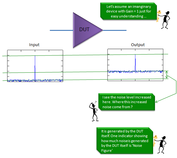
- The DUT is drawn as an amplifier with Gain = 1, so the signal peak has the same height in the Input plot and in the Output plot.
- The green lines mark the levels. The noise floor of the Output plot sits clearly above the noise floor of the Input plot, and the green arrow on the right marks the difference.
- The notes on the right ask where the increased noise comes from, and answer that the DUT generates it itself.
Where does this internal noise physically come from? The main source is thermal noise. Every resistor and every lossy part of a transistor contains electrons that move randomly, and the strength of that motion grows with temperature. The random motion appears as a noise voltage at the terminals. Active devices add further noise on top of it, for example shot noise from the discrete charges that cross a junction and flicker noise at low frequency. Noise figure does not separate these mechanisms. It combines all of them into one number, and that number says how much the device degrades the signal to noise ratio.
Noise figure measures only the noise the device adds itself : noise that arrives at the input together with the signal is not part of it.Every device above absolute zero adds some noise : thermal noise comes from the random motion of electrons, so even a passive part with loss adds noise.A higher output noise floor with an unchanged signal peak points to internal noise : the unity gain example shows exactly this pattern.
Why is noise factor defined with SNR ?
As soon as a device has gain, a noise level alone cannot tell us how much noise the device added. The amplified input noise and the added noise appear together at the output. So we need a measure that stays fair when the signal and the input noise are amplified by the same gain, and the SNR is that measure.
How can we express this noise figure in formal way ? If the gain of the device is always 1, the simplest way to express it would be the 'difference between input noise level and output noise level'. But if the Gain is not 1 (greater than 1), just looking at the noise level difference you don't know whether the increased noise level is due to the amplification or internal generation. In this case, the better way to estimate the internal noise generation is to compare SNR (signal to noise ration) as shown below.
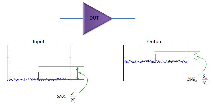
In conclusion, they came out with an indicator called 'Noise Factor' which is defined as the ratio of input SNR and output SNR' as shown below.
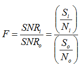
Noise figure is just log scaled value of Noise Factor as shown below.

Let's read the two formulas with numbers. Suppose the input SNR is 20 dB and the output SNR is 17 dB. The noise factor is then 102.0 / 101.7, which is about 2.0, and the noise figure is 10 log(2.0) = 3 dB. In dB the calculation is a plain subtraction, NF = SNRi - SNRo, with both SNR values in dB.
A device cannot improve the SNR of the signal that passes through it. It amplifies the signal and the input noise by the same gain, and it can only add noise of its own. So F is never less than 1, and NF is never less than 0 dB. An ideal noiseless device has F = 1 and NF = 0 dB.
The definition carries one condition. The measured F depends on how much noise arrives at the input, so the standard definition fixes the input noise as the thermal noise of a matched source at 290 K. The section on noise temperature below explains this reference.
Noise factor is the ratio SNRi / SNRo : it compares the SNR before and after the device, so the gain cancels out of the comparison.Noise figure is the same quantity in dB : NF = 10 log(F), which equals SNRi - SNRo when both are written in dB.F is at least 1 and NF is at least 0 dB : a real device can keep the SNR at best, and in practice it always reduces the SNR a little.
How is noise factor derived from gain and added noise ?
The SNR ratio defines noise factor, but it hides the noise the device adds. Let's open the ratio and write it in terms of the gain G, the input noise Ni and the added noise Na. The result shows directly what a given noise figure means in noise power.
This is all about the noise figure, but if you want to play more with math. Noise Factor can be derived from the Gain (G), input noise (Ni) and the internally generated noise (Na) as shown below.
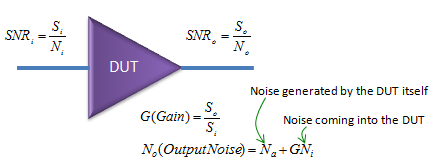
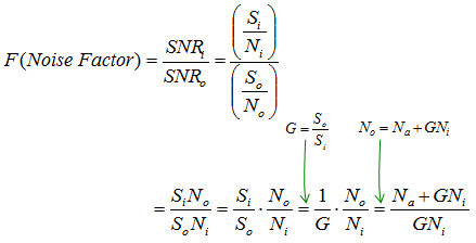
Whatever the way you use, once you get noise factor, getting the noise figure (NF) is automatic. Just take the log scale of it as shown below.
Let's read the result term by term. The derivation ends with F = (Na + G Ni) / (G Ni), and this is the same as F = 1 + Na / (G Ni). The 1 stands for the input noise, which the device only amplifies. The second term compares the added noise with the amplified input noise. If the device adds nothing, the second term is zero and F = 1.
We can also divide Na by G. This moves the added noise back to the input, and Na / G is called the input referred noise. Then F = 1 + (Na / G) / Ni. In this form devices with very different gains can be compared directly, because each one is judged against the same input noise.
Now let's put numbers into it. Take an amplifier with G = 20 dB and a bandwidth of 1 MHz. The thermal input noise in 1 MHz is Ni = -114 dBm, so the amplified input noise G Ni is -94 dBm at the output. Suppose the device adds Na of the same size, -94 dBm. The output noise then doubles to -91 dBm, F = 1 + 1 = 2, and NF = 3 dB. So a 3 dB noise figure means that the device adds as much noise as the amplified thermal noise of its input.
F = 1 + Na / (G Ni) : the 1 is the input noise, and the second term is the added noise compared with the amplified input noise.Input referred noise makes devices comparable : Na / G is the added noise moved back to the input, so the gain of each device no longer matters for the comparison.NF = 3 dB means F = 2 : the device adds exactly as much noise as the amplified thermal input noise, and the output noise is twice the noiseless value.
What are noise temperature and the 290 K reference ?
The previous sections used Ni without saying how large it is. That matters, because the same device shows a different F when the input noise changes. So the definition needs a fixed input noise, and engineers express it as a temperature.
A resistor at temperature T delivers the available noise power N = k T B into a matched load. Here k is the Boltzmann constant, 1.38 x 10⁻²³ J/K, and B is the bandwidth in Hz. The standard reference temperature is T0 = 290 K, which is close to room temperature. At T0 the noise density is k T0 = 4.0 x 10⁻²¹ W/Hz, or about -174 dBm/Hz. In a 1 MHz bandwidth the noise power is -174 + 60 = -114 dBm, which is the Ni used in the example above.
The added noise of a device can be described in the same way. Imagine a resistor at the input whose thermal noise, amplified by G, equals Na. Its temperature is the equivalent noise temperature Te, so Na / G = k Te B. Putting this into the result of the previous section gives F = 1 + Te / T0, or Te = T0 (F - 1). The table below converts a few noise figures.
NF, dB | F, linear | Te = 290 (F - 1), K |
0.5 | 1.122 | 35.4 |
1 | 1.259 | 75.1 |
2 | 1.585 | 169.6 |
3 | 1.995 | 288.6 |
6 | 3.981 | 864.5 |
10 | 10.000 | 2610.0 |
Notice how the table spreads out near 0 dB. The step from 0.5 dB to 1 dB is only half a dB in noise figure, but Te more than doubles. This is why datasheets for very low noise amplifiers, such as those for satellite receivers, often quote noise temperature rather than noise figure. Also notice that NF = 3 dB gives Te of about 290 K. It is the same statement as in the previous section: the device adds as much noise as the reference input noise.
A passive part with loss is a special case. A matched attenuator or cable at 290 K with a loss L has F = L. So its noise figure in dB equals its loss in dB, and a 2 dB cable has NF = 2 dB.
The reference input noise is k T0 B with T0 = 290 K : it is about -174 dBm/Hz, or -114 dBm in 1 MHz.Te = T0 (F - 1) : noise temperature and noise factor carry the same information, and noise temperature resolves low noise devices better.A lossy passive part at 290 K has NF equal to its loss : a cable or filter in front of a receiver adds its full loss to the noise figure.
How does noise figure add up in a cascade ?
A real receiver is a chain of stages, for example an LNA, a mixer and an IF amplifier. Each stage has its own gain and noise figure. So we need a rule that combines them into one noise figure for the whole chain, and the rule also tells us which stage matters most.
The rule is the Friis formula for noise. It is written with linear noise factors and linear gains, never with dB values.
Ftotal = F1 + (F2 - 1) / G1 + (F3 - 1) / (G1 G2) + ...
Each stage after the first contributes its excess noise F - 1, divided by the total gain in front of it. This follows from the input referred noise of the previous section. The noise that stage 2 adds is moved back to the chain input through G1, so it shrinks by the factor G1. Figure 1 applies the formula to a three stage chain with an LNA of 20 dB gain in front.
Figure 1. Noise figure of a three stage chain. The LNA contributes almost all of the total noise factor, because its 20 dB gain divides the noise of every later stage. The 10 dB mixer adds only 0.09 to F.
- Each box shows the linear values used in the formula after conversion: G1 = 100, F1 = 1.413, G2 = 0.1995, F2 = 10 and F3 = 2.512.
- The terms under the boxes add up to Ftotal = 1.578, which is NFtotal = 1.98 dB. The chain is only about 0.5 dB worse than the LNA alone.
- The mixer has a loss of 7 dB, so the IF amplifier behind it is divided by G1 G2 = 19.95 rather than by 100.
Now let's change the order and see what happens. If the mixer comes first and the LNA second, with the same three stages, the total noise figure becomes 10.84 dB. The 10 dB noise figure of the mixer now sits in the F1 position, where nothing divides it. Next, let's put a 2 dB cable in front of the original chain. The cable has F1 = L and G1 = 1/L, so it multiplies the noise factor of everything behind it by L. The total noise figure becomes 1.98 + 2 = 3.98 dB. This is the reason an LNA is placed as close to the antenna as possible.
The Friis formula uses linear values : convert every NF and gain from dB before adding the terms, and convert the result back at the end.The first stage sets the noise figure of the chain : its gain divides the excess noise of every later stage.Loss in front of the LNA adds directly to the noise figure : a 2 dB cable before the LNA raises the chain NF by 2 dB.
How does noise figure set receiver sensitivity ?
Why does a receiver designer care about one or two dB of noise figure? The answer is sensitivity, the weakest signal the receiver can still demodulate. Noise figure enters the sensitivity calculation directly, dB for dB.
Let's build the calculation in three steps. The first step is the thermal noise at the input, -174 dBm/Hz. The second step scales it to the receiver bandwidth by adding 10 log(B). The third step adds the noise figure, because the receiver degrades the SNR by NF. The result is the effective noise floor of the receiver, referred to its input. The receiver still needs some minimum SNR to demodulate the signal, so the sensitivity is that noise floor plus the required SNR.
Sensitivity, dBm = -174 + 10 log(B) + NF + SNRmin
Let's take B = 9 MHz, which is the occupied bandwidth of a 10 MHz LTE carrier with 50 resource blocks. Then 10 log(9 x 10⁶) = 69.5 dB, and the thermal noise in that bandwidth is -174 + 69.5 = -104.5 dBm. With NF = 9 dB the receiver noise floor is -95.5 dBm. If the demodulator needs an SNR of 0 dB, the sensitivity is also -95.5 dBm. Every dB taken off the noise figure moves the sensitivity down by one dB.
Sensitivity = -174 dBm/Hz + 10 log(B) + NF + SNRmin : noise figure is one of four terms, and it is the one the RF design controls.One dB of NF is one dB of sensitivity : a lower noise figure lets the receiver work with a weaker signal, and so at a longer range.The LNA and the loss in front of it decide the NF : the cascade rule of the previous section shows why.