Amplifier is a device which turn 'something' small into 'something' larger. It is like a magnfying glass. What does this amplify ? it normally amplify (magnify) current or voltage or power as shown below.
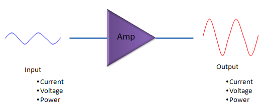
Following is the list of topics I will go through in this note.
- Types of RF Power Amplifier
- Ideal vs. Real Amplifier
- Why Non-Linearity is issue ?
- How do we represent the degree of non-linearity ?
- How can we avoid Non-Linear Effect ?
- Gain vs Efficiency
Types of RF Power Amplifier
These days it seems to get harder and harder to find applications/products which is using amplifiers as a separate component (discrete component) and as a result I found it difficult to find engineers who has such an experiences of dealing with discrete amplifier. In most product especially mobile communication product (e.g, mobile phone, smartphone), most of the amplifiers (especially reciever chain amplifiers) are integrated into various RF ICs. One of few cases, you still see a discrete amplifier (like (a)~(e)) would be final stage power amplifier of transmitter chain. The reason why you cannot integrate this power amplifier into RF IC is that it is generating so much heat.
In some other applications where you can still see discrete amplifier (or a module in which a couple of discrete amplifiers are the main component like (f)~(k)) would be a system which requires very high power transmission (e.g, telecommunication repeater, various base station for mobile communication system).
Very recently even such a high power amplifiers start getting equipped with various control circuit and interface (e.g, eithernet) and can be installed right next to the antenna located on top of high towers (e.g, base station). This kind of amplifier (actually, I can call it an amplifier system) is called Remote Radio Head(e.g, (l),(m)).
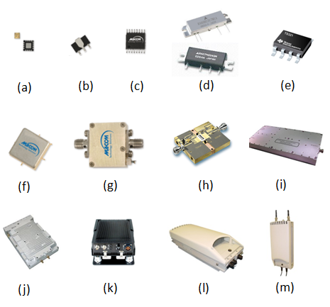
Amplifiers come as bare ICs, as connectorized modules and as complete remote radio heads. The higher the output power, the larger the package, mostly because of the heat it has to remove.
(a) to (e) are single devices : small packaged amplifiers and power transistors that are soldered onto a circuit board.(f) to (k) are modules : housed amplifiers with coaxial connectors or large heat sinks, as used in repeaters and base stations.(l) and (m) are remote radio heads : outdoor units that combine the power amplifier with control circuits and an interface, installed next to the antenna.
The word type has a second meaning in amplifier design, and it matters more for the rest of this page. Power amplifiers are also grouped by class. The class says how the transistor is biased, and that decides for how much of each RF cycle the transistor conducts. The fraction of the cycle is called the conduction angle, where a full cycle is 360 deg. A smaller conduction angle wastes less DC power, but it distorts the signal more.
The table below gives the ideal maximum drain efficiency for each class. These numbers assume ideal transistors and a load tuned to the fundamental. Real amplifiers reach less than this.
Class |
Conduction angle |
Ideal maximum efficiency |
Linearity |
Typical use |
A |
360 deg |
50 % |
Best |
Low power linear stages, driver stages |
AB |
Between 180 and 360 deg |
Between 50 and 78.5 % |
Good |
Most linear PAs for LTE and NR |
B |
180 deg |
78.5 %, which is π/4 |
Moderate |
Push-pull stages |
C |
Below 180 deg |
89.7 % at 120 deg, and toward 100 % as the angle falls |
Poor |
Constant envelope signals such as FM |
D, E, F |
Switching |
100 % in theory |
Needs linearization |
Switch-mode and envelope tracking designs |
A cellular transmitter carries a signal whose amplitude changes all the time, so a class C or a switching amplifier cannot pass it alone. That is why most handset and base station PAs are class AB, which keeps an acceptable linearity and a reasonable efficiency. The receiver side is different. A low noise amplifier, LNA, handles tiny signals, and its main figure of merit is the noise figure rather than the efficiency.
A PA is still one of the few discrete amplifiers : it produces too much heat to share a die with the rest of the RF IC.The amplifier class trades linearity for efficiency : class A wastes the most DC power, and class C and the switching classes distort the most.Class AB is the usual choice for LTE and NR : the signal has a varying envelope, so the PA has to stay reasonably linear.PA and LNA are optimised for different things : the PA for output power and efficiency, the LNA for noise figure.
Ideal vs. Real Amplifier
Ideal function of an amplifier is very simple. If you express the function in the form of mathematical expression, it would look even simpler. The ideal function is to implement some of the simplest mathematical function (f(x) = a x, where a > 1) as expressed in blue straight line in the following graph.
However, as I know, as you know, as everybody experienced, nothing goes like theory. In reality, the characteristics of an amplifies goes as shown in red. In this curve, in some section you would see a straight line which is very close to ideal operation, but from some point the behavior deviates from the ideal operation. Mathematically this non-ideal (non linear) curve can be represented in a polynomial as shown below.
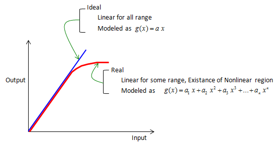
An ideal amplifier is one coefficient. A real amplifier needs a polynomial, because its gain changes with the input level.
The blue line is g(x) = a x : the output is the input multiplied by a constant, for every input level.The red curve is g(x) = a1x + a2x2 + a3x3 + ... + anxn : at small inputs the higher powers of x are negligible, so the curve follows the blue line.The red curve flattens at large inputs : the flat part is saturation, where the output stops growing.
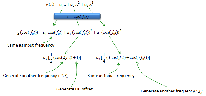
Each coefficient of the polynomial has its own job. The coefficient a1 is the small-signal gain, the slope of the blue line. The coefficient a2 belongs to the even-order term. It creates a DC offset and signals at twice the input frequency, as the next section shows. The coefficient a3 belongs to the odd-order term. When a3 has the opposite sign to a1, it reduces the output at the input frequency as the input grows. That is the bend of the red curve, which the 1 dB compression point measures.
The polynomial is a memoryless model. It assumes the output depends only on the input at the same instant. Wideband power amplifiers also show memory effects, where the output depends on recent inputs as well, for example because of heating or bias circuits. The polynomial is still the right starting point, because it explains which new frequencies appear and where.
a1 is the gain : it is the only coefficient an ideal amplifier has.a3 causes compression : with the sign opposite to a1, the third-order term lowers the output at the input frequency.The model has no memory : it explains new frequencies well, but it cannot describe effects that depend on the history of the signal.
Why Non-Linearity is issue ?
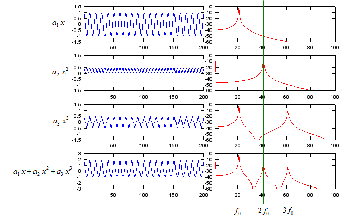
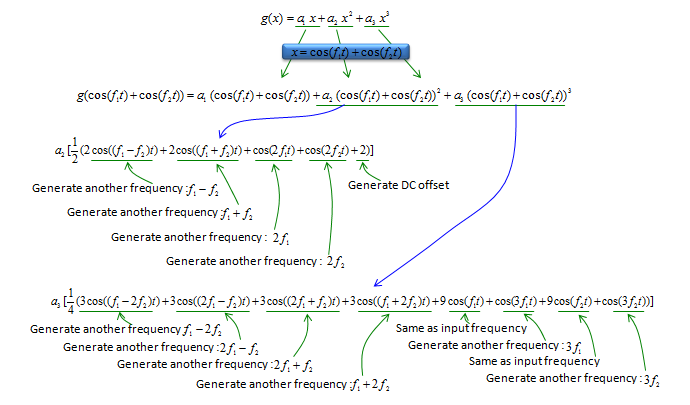
Then your question would be "Why these non-linear portion matters ?", "Does it cause any problem ?". This problem can easily explained by simple math that you learned in high school. Let's assume that we have an amplifier which has characteristics of g(x) as shown below and you put a very simple signal represented as cos(f t). By a couple of mathematical steps, you can get the following expression. (if you are not so good at math or too lazy to calculate this as me, just try with Wolfram Alpha). Important thing is not the calculation process (you can always let Software do it). it is more important to understand how to interpret the result. From the result, you would see a couple of different frequencies which does not exists in the input signal (cos(f0 t)). It means that the main problem of non-linearity of the amplifier is that it produces many additional frequencies which we don't like to have.
If you prefer graphical expression to the dry mathematical expression like me, here goes what you like. The first row of the graph shows the ideal operation of the amplifier and the last row shows the result of the amplifier with the second and the third order of polynomials (non linear portion), here you see two additional frequency spikes which does not exists in the input signal. The second and third row shows separate plots for second and third order only for your understanding.
If you put into a composite signal (a signal composed of two frequencies in this example), you would have more complicated result as shown below due to non-linear properties of the amplifier. For sure, I used the software to solve this equation -:), I don't want to spend half an hour pulling my hair this solve this on my own -:). What is the implication of the result ? Simple !!! you got hell lots of additional frequencies that you don't want !!
If I plot the mathematical expression into a graph, I get following result. If you are testing a real amplifier, it is important to figure the exact locations of the spikes in frequency domain which are generated by this non-linearity. If you measure the amplifier characteristics with spectrum analyzer or network analyzer, you will see a lot of other spikes which has not input to the amplifier. Some of the spikes would have been generated by this non linearity and some other spikes would have been generated by other causes. So understanding the effect of this non linear characteristics would help you figure out the source of those unwanted spikes in frequency domain.
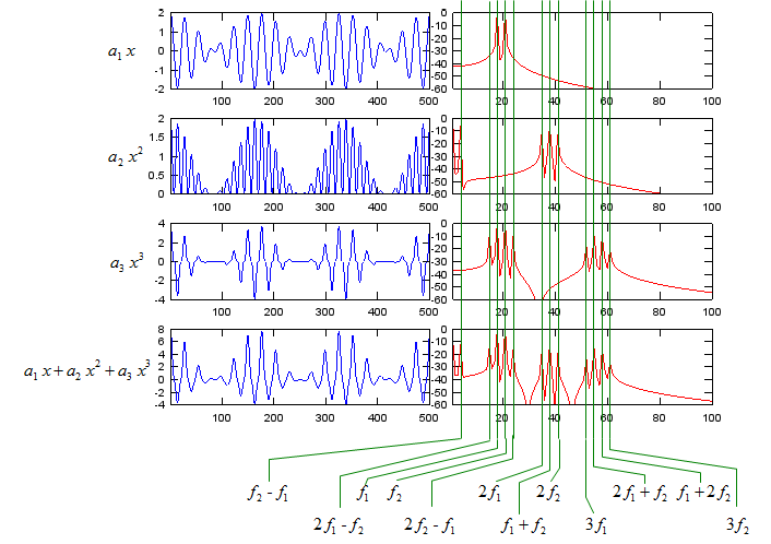
If the input signal to Amplifier is very narrow bandwidth or CW signal, you would have to issues as described above by non-linearity of the amplifier. However, you would have more cases where you put modulated wideband signal as the input to the amplifier, in this case the most obvious side effect caused by the non linearity would be poor ACLR/ACPR.
Let's put numbers on the two-tone result, because the location of each product decides how hard it is to remove. Take two tones at f1 = 1000 MHz and f2 = 1001 MHz, 1 MHz apart. The table below lists the products that the second-order and third-order terms create.
Product |
Created by |
Frequency |
Distance from the wanted tones |
f2 - f1 |
a2 |
1 MHz |
Far below |
2f1, f1 + f2, 2f2 |
a2 |
2000, 2001, 2002 MHz |
Around the second harmonic |
2f1 - f2 |
a3 |
999 MHz |
1 MHz below f1 |
2f2 - f1 |
a3 |
1002 MHz |
1 MHz above f2 |
2f1 + f2, f1 + 2f2 |
a3 |
3001, 3002 MHz |
Around the third harmonic |
3f1, 3f2 |
a3 |
3000, 3003 MHz |
Third harmonic |
Most of the products land far from the wanted tones, so a filter after the amplifier can remove them. Two products cannot be removed that way. 2f1 - f2 and 2f2 - f1 sit only one tone spacing away from the wanted signal, inside the band that the filter has to pass. These are the third-order intermodulation products, IM3. A modulated signal behaves like many tones at once, so its IM3 products fill the channel and the space right beside it. That is the spectral regrowth measured as ACLR.
The size of the products follows from the expansion. For two equal tones of amplitude 1, the a3 term adds 9/4 a3 at each wanted tone and 3/4 a3 at each IM3 frequency. Both grow with the cube of the input amplitude. So when the input rises by 1 dB, the IM3 products rise by 3 dB, while the wanted output rises by only 1 dB.
Second-order products are far away : f2 - f1 and the products near 2f are easy to filter, and a differential circuit also suppresses them.IM3 products sit next to the wanted signal : 2f1 - f2 and 2f2 - f1 are one tone spacing away, so no filter can remove them without removing the wanted signal too.IM3 grows 3 dB for every 1 dB of input : the gap between the wanted signal and IM3 closes by 2 dB for every 1 dB of extra drive.A modulated signal turns IM3 into regrowth : the many products of a wideband signal merge into shoulders on each side of the channel.
How do we represent the degree of non-linearity ?
Generally speaking, 'Non linear characteristics' is not good in amplifier and these are something that we want to avoid, but never can remove completely. In most case, if there is something that we don't like and try to remove it as much as possible, we make some 'indicator' of those property and put them in the datasheet (specification sheet).
As you can guess, we have some indicator in the specification of an amplifier which represents those nonlinear properties of the amplifier. The most common indicators are IP3 (Third order intercept point) and 1 dB compression point.
The two indicators look at the same nonlinearity from two ends. The 1 dB compression point, P1dB, is the input or output power where the gain has dropped 1 dB below its small-signal value. It describes the effect of a3 on the wanted signal itself. IP3 describes the effect of a3 on the IM3 products. It is the power where the extrapolated IM3 line, with its slope of 3, would meet the extrapolated wanted-signal line, with its slope of 1. No amplifier actually reaches that point, so IP3 is always found by extrapolation.
The output-referred intercept, OIP3, gives the IM3 level directly. For two equal tones, each at output power Pout in dBm, each IM3 product is at PIM3 = 3Pout - 2 OIP3. For example, an amplifier with OIP3 = +40 dBm and Pout = +10 dBm per tone gives PIM3 = 30 - 80 = -50 dBm. That is 60 dBc below each tone, which is 2 x (OIP3 - Pout). If the same amplifier runs 5 dB hotter, the IM3 products come up by 15 dB and the ratio shrinks to 50 dBc.
For a pure third-order polynomial, the input-referred IP3 is 9.64 dB above the input-referred P1dB. This link holds only for the model. Real amplifiers depart from it, so a data sheet quotes both numbers from measurement. For modulated signals, system-level indicators take over, mainly ACLR/ACPR for the leakage outside the channel and EVM for the distortion inside it.
P1dB measures compression of the wanted signal : it is a real operating point that can be measured on a power sweep.IP3 measures the growth of IM3 products : it is an extrapolated point that no amplifier actually reaches.PIM3 = 3Pout - 2 OIP3 : so the ratio between each tone and its IM3 product is 2 x (OIP3 - Pout).ACLR and EVM are the indicators for modulated signals : they measure distortion outside and inside the channel for the actual waveform.
How can we avoid Non-Linear Effect ?
The previous sections showed that the distortion cannot be removed from inside the amplifier. So every remedy works around it, either by keeping the signal out of the nonlinear region, by removing the products afterwards, or by distorting the input in advance. Each remedy costs something: power, efficiency, components or processing.
Now you may have one question as below.

There is no way you can remove this issues completely, but there are various ways to reduce the problem. As far as I understand, there are a couple of common techniques as shown below.
First way you can think of is just to replace one amplifier with another one which has wider linear regions as shown at the top. But it usually require additional cost and in some case those components would not exists at all.
Another method is to shift the level of the signal to a little bit lower power region so that it operates in linear region of the amplifier characteristic curve. But this method cannot be applied when the amplitude of the signal is so wide (backoff is large) and there is not much room to shift.
Another method is just let the amplifier to produce all those dirty spikes and filter those unwanted spikes with additional filters. This method also requires additional cost and in some case you may find difficulties to find proper filter which can handle such a high power (amplified signal).
There is another method which is developed recently and is used in some advanced application. It is a technology called Predistortion. It is smart and advanced technique, but figuring out proper algorithm for predistortion is tricky job.
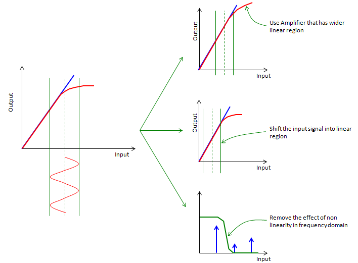
Three ways to reduce the nonlinear effect. The first two keep the signal swing inside the linear region, and the third removes the products after they are created.
The left graph is the problem : the input swing between the two green lines reaches past the dashed line into the bend of the red curve, so part of the signal is distorted.The top graph uses an amplifier with a wider linear region : the red curve now bends only beyond the signal swing.The middle graph shifts the input into the linear region : the same swing now sits lower on the curve and stays below the bend. In RF terms this is output power back-off.The bottom graph filters the output : a low pass filter keeps the wanted spike and suppresses the spikes at higher frequencies.
The filter panel has a limit that the two-tone table above makes clear. A filter removes harmonics and other far-away products. It cannot remove IM3 products, because they sit right beside the wanted signal. So filtering helps against harmonic emissions, while back-off, a more linear amplifier or predistortion is needed against ACLR. Back-off has a price too. The IM3 products fall by 3 dB for each 1 dB of back-off, but the efficiency falls as well, as the next section shows.
Back-off is the simplest remedy : each 1 dB of back-off improves the signal-to-IM3 ratio by about 2 dB.Filters cannot remove in-band distortion : they help against harmonics, not against IM3 or spectral regrowth.Predistortion corrects the distortion before it happens : it lets the amplifier run closer to compression, so it keeps more of the efficiency.
Gain vs Efficiency
As I mentioned above, amplifier is a device which make a small input signal (energy) a big output signal(energy). It mean the amplifier is supplying high amount of energy to the incoming signal. Then where the amplifier is getting the energy ? It is provided by external energy source marked as 'Vdd' shown below. In case of your mobile phone, this Vdd would be connected to the battery and in a big system like base station, this part will be eventually connected to external power line.
The term Gain represents how much the amplifier magnifies the input signal which means the ratio between input signal and output signal power.
The term Efficiency represents with how small energy the amplifier can achieve its desired amplication. For example, when you have to amplifier A and B with the same gain. Amplierfier A achieves that gain with 3 V, 100 mA and B achieves the same gain with 4.2V, 200 mA. You can say Amplifier A is more efficient than the amplifier B. Another way of expressing Efficiency would be "how little energy an amplifier waste in the amplication process". Amplifier with low efficiency means that it waste more engergy during the amplification. Where the wasted engergy would go ? it goes out as heat.
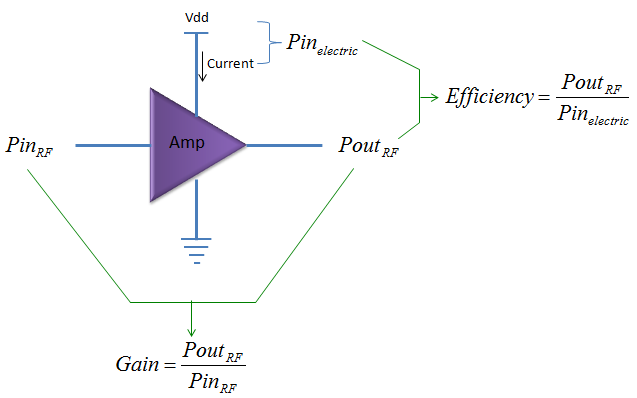
Gain compares RF output with RF input. Efficiency compares RF output with the DC power drawn from Vdd.
Gain = PoutRF / PinRF : both powers are RF powers. In dB, gain is PoutRF in dBm minus PinRF in dBm.Efficiency = PoutRF / Pinelectric : Pinelectric is the DC power, Vdd multiplied by the supply current. This ratio is called drain efficiency, or collector efficiency for a bipolar transistor.The two ratios are independent : an amplifier can have a high gain and a poor efficiency, or the other way round.
A second efficiency figure is common on PA data sheets. Power added efficiency, PAE, subtracts the RF input from the RF output, PAE = (PoutRF - PinRF) / Pinelectric. It gives credit only for the power the amplifier adds. For a high-gain stage PAE and drain efficiency are almost equal, and for a low-gain stage PAE is noticeably lower.
Let's work one example. A handset PA delivers +28 dBm, which is 0.631 W, from a 3.4 V supply drawing 0.5 A. The DC power is 1.7 W, so the drain efficiency is 0.631 / 1.7 = 37.1 %. With a gain of 25 dB the input is +3 dBm, or 2 mW. PAE is then (0.631 - 0.002) / 1.7 = 37.0 %. The rest, about 1.07 W, leaves the PA as heat.
Efficiency also depends on how far the amplifier is backed off. The ideal efficiency of a class A amplifier falls in proportion to the output power, and that of a class B amplifier in proportion to the output amplitude. At 6 dB of back-off, class A drops from 50 % to 12.6 %, and class B drops from 78.5 % to 39.4 %. This is the cost of the back-off remedy in the previous section, and it is why signals with a high peak-to-average power ratio are hard on battery life.
PAE counts only the power the amplifier adds : PAE = (PoutRF - PinRF) / Pinelectric.Wasted DC power becomes heat : in the example, 1.07 W of the 1.7 W drawn from the supply heats the PA.Back-off costs efficiency : 6 dB of back-off halves the ideal efficiency of class B and quarters that of class A.Linearity and efficiency pull in opposite directions : this trade is the reason for class AB bias, envelope tracking and predistortion.